
“`html
Nanostructures represent a remarkable assortment of complex designs that are invisible to the naked eye, yet they play a crucial role in contemporary existence. They serve as the foundational components of microchip transistors, inscribed onto patterned substrates of extraterrestrial X-ray telescopes, and are essential in driving advancements in healthcare, environmental sustainability, and quantum computing.
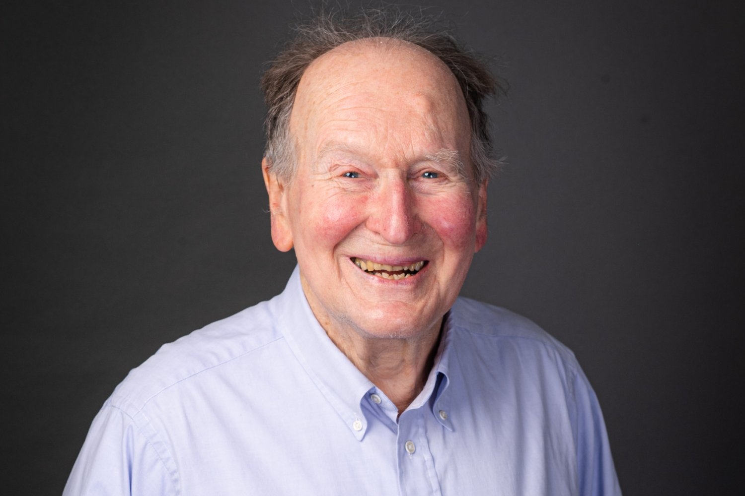
Since the 1970s, Henry “Hank” Smith, professor emeritus of electrical engineering at MIT, has been a prominent figure in this domain. He initiated the application of proximity X-ray lithography, demonstrating that the brief optical wavelength of X-rays could yield high-definition patterns at the nanometer level. Smith also achieved notable progress in phase-shifting masks (PSMs), a methodology that alters light waves to improve contrast. His creation of attenuated PSMs, co-developed with graduate students Mark Schattenburg PhD ʼ84 and Erik H. Anderson ʼ81, SM ʼ84, PhD ʼ88, remains in use today within the semiconductor sector.
In acknowledgment of these achievements, along with impactful contributions to liquid-immersion lithography, achromatic-interference lithography, and zone-plate array lithography, Smith recently was honored with the 2025 SPIE Frits Zernike Award for Microlithography. Awarded by the Society of Photo-Optical Instrumentation Engineers (SPIE), this recognition celebrates researchers for their exceptional contributions to microlithographic technologies.
“The Zernike Award is a formidable accolade that fittingly honors Hank’s innovative contributions,” states Karl Berggren, MIT’s Joseph F. and Nancy P. Keithley Professor in Electrical Engineering and head of the electrical engineering faculty. “Whether in the classroom, at a research symposium, or in the lab, Hank approached his work with immense scientific rigor that placed him light-years ahead of industry standards.”
At 88 years young, Smith has received numerous other accolades. He has also been honored with the SPIE BACUS Prize, elected to the National Academy of Engineering, and is a fellow of the American Academy of Arts and Sciences, IEEE, the National Academy of Inventors, and the International Society for Nanomanufacturing.
Launching the nano frontier
From an early age, Smith was captivated by the environment around him. He disassembled clocks to understand their mechanisms, explored nature, and even observed the flow of water. After completing high school in New Jersey, Smith pursued a degree in physics at the College of the Holy Cross. Subsequently, he sought his doctorate at Boston College and served three years as an officer in the U.S. Air Force.
It was his position at MIT Lincoln Laboratory that ultimately transformed Smith’s career path. There, he encountered visitors from MIT and Harvard University who shared their ambitious concepts for electronic and surface acoustic wave devices but were hindered by the physical constraints of fabrication. However, few were motivated to address this challenge.
“The task of creating things was often dismissed with, ‘oh well, we’ll have some technicians handle that,’” Smith noted in his oral history for the Center for Nanotechnology in Society. “And the intellectual aspects of fabrication technology weren’t valued by those who had been ‘traditionally educated,’ I suppose.”
More focused on problem-solving than preserving academic hierarchy, Smith endeavored to comprehend the science of fabrication. His breakthrough in X-ray lithography highlighted to the world the potential and opportunities of operating at the nanoscale, according to Schattenburg, who is a senior research scientist at MIT Kavli Institute for Astrophysics and Space Research.
“His early efforts demonstrated to individuals at MIT and researchers nationwide that nanofabrication possessed merit,” Schattenburg states. “By illustrating what was achievable, Hank truly ignited the nano frontier.”
Uncovering lithography’s enigma
By 1980, Smith departed Lincoln Lab for MIT’s primary campus and continued to advance new concepts in his NanoStructures Laboratory (NSL), which was previously the Submicron Structures Laboratory. NSL functioned as both a research facility and a service center that supplied optical gratings—pieces of glass carved with sub-micron recurring designs—to the MIT community and external scientists. It was a bustling period for the lab; NSL attracted graduate students and global visitors. Nevertheless, Smith and his team ensured that everyone visiting NSL would also receive an introduction to nanotechnology.
“Hank never wished for anything we produced to be seen as a black box,” remarks Mark Mondol, MIT.nano e-beam lithography expert who collaborated with Smith in NSL for 23 years. “Hank was always eager for people to grasp our work and its processes, and he was the ideal individual to elucidate it as he communicated in straightforward and accessible terms.”
The physical NSL space in MIT Building 39 closed in 2023, a decade after Smith attained emeritus status. The knowledgeable staff and unique capabilities of NSL transitioned to MIT.nano, which now acts as MIT’s central hub for promoting advancements in nanoscience and nanotechnology. Undeterred, Smith continues to share his insights with the ever-growing nano community by delivering talks at the NSL Community Meetings at MIT.nano that focus on lithography, nanofabrication, and their future.
Smith’s journey is far from over. Through his startup LumArray, he continues to extend the boundaries of understanding. He recently developed a maskless lithography technique called X-ray Maskless Lithography (XML), which has the potential to reduce manufacturing expenses for microchips and combat the trade of counterfeit microchips.
Dimitri Antoniadis, professor emeritus of electrical engineering and computer science at MIT, is Smith’s long-time collaborator and friend. He notes that Smith’s dedication to research is nearly unparalleled.
“Once professors achieve emeritus status, we typically guide and oversee research,” Antoniadis explains. “It’s quite unusual for retired professors to undertake all the work themselves, but he enjoys it.”
Lasting influence
Smith’s impact stretches far beyond the innovative tools and methods he has developed, as expressed by his friends, colleagues, and former students. His insatiable curiosity and dedication to his graduate students have propelled his field forward.
He earned a reputation for sitting in the front row at research symposia, poised to pose the first question. Fellow researchers sometimes dreaded his presence there.
“Hank kept us accountable,” Berggren remarks. “Scientists and engineers knew they couldn’t make assertions that were overstated or use evidence that didn’t support the hypothesis, for Hank would hold them responsible.”
Smith never perceived himself as playing the good cop or bad cop—he was merely a curious learner unafraid to appear foolish.
“There are renowned individuals, Nobel laureates, who will attend research presentations and have no clue about what’s taking place,” Smith states. “That is a complete waste of time. If I don’t comprehend something, I’m going to inquire.”
As an advisor, Smith upheld high standards for his graduate students. If they arrived unprepared or lacked comprehension of their research, he would challenge them with probing, relentless inquiries. Yet he was also their staunchest supporter, helping students like Lisa Su SB/SM ʼ91, PhD ʼ94, now chair and chief executive officer of AMD, and Dario Gil PhD ʼ03, currently chair of the National Science Board and senior vice president and research director at IBM, thrive in the lab and beyond.
Research Specialist James Daley has dedicated nearly thirty years to MIT, primarily working alongside Smith. Throughout that time, he has witnessed countless advisees graduate and return to express their gratitude. “Hank’s former students are dispersed across the globe,” Daley says. “Many are now professors mentoring their own graduate students, carrying forth some of Hank’s approach. They are his most significant legacy.”
“`