
“`html
MIT scholars have created a method that facilitates real-time, 3D observation of corrosion, fractures, and other material failure phenomena within a nuclear reactor context.
This could enable engineers and researchers to engineer safer nuclear reactors that also provide enhanced performance for uses such as electricity production and naval vessel propulsion.
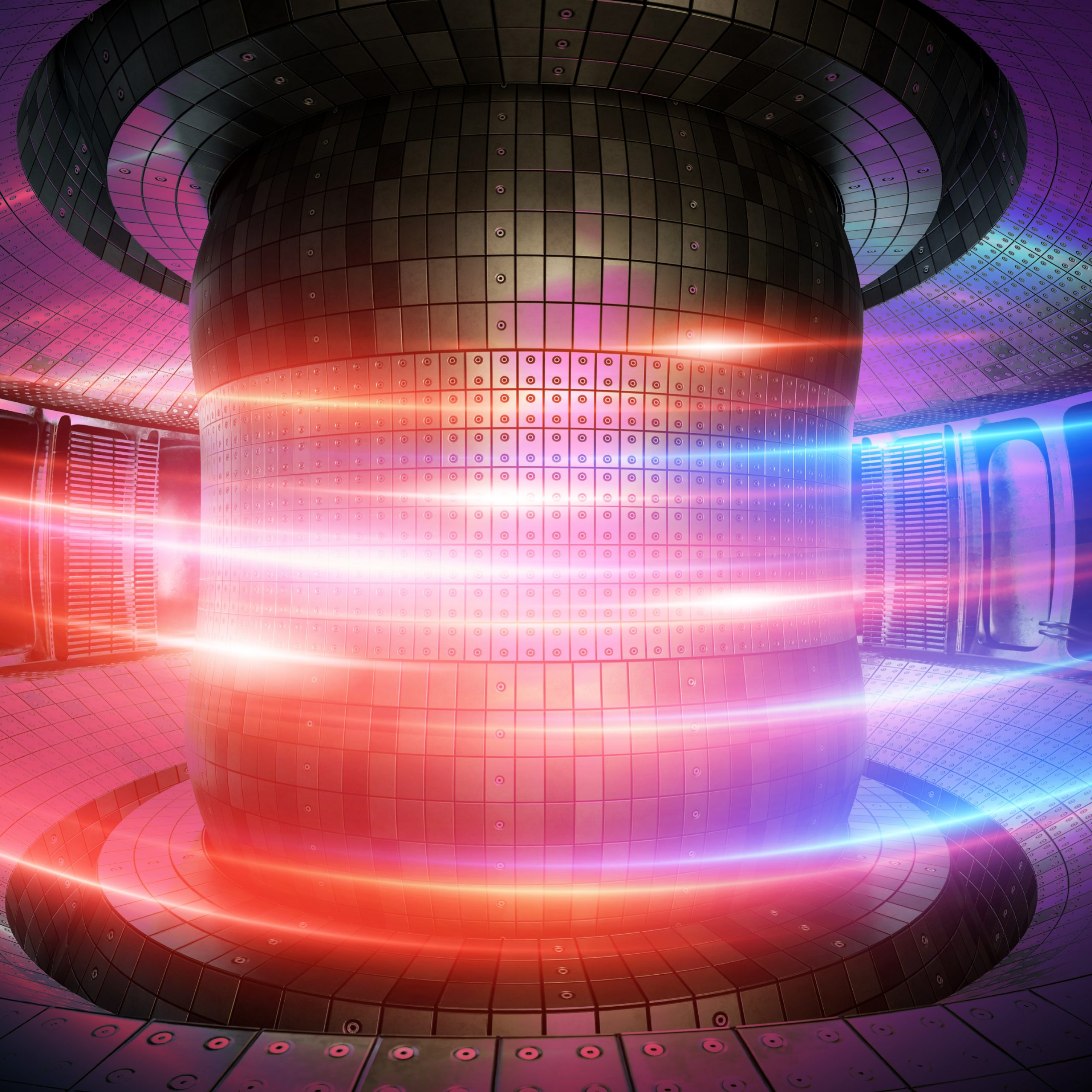
Throughout their trials, the scholars employed extraordinarily powerful X-rays to replicate the interactions of neutrons with materials inside a nuclear reactor.
They discovered that introducing a silicon dioxide buffer layer between the material and its substrate, along with extending the exposure time to the X-ray beam, enhances the sample’s stability. This evolution enables real-time surveillance of material failure phenomena.
By reconstructing 3D image data on a material’s structure as it deteriorates, researchers could devise more robust materials that better endure the stresses introduced by irradiation within a nuclear reactor.
“If we can enhance materials utilized in a nuclear reactor, we can prolong the reactor’s lifespan. It also implies that materials will take longer to fail, allowing us to maximize the utility of a nuclear reactor compared to our current usage. The method we’ve introduced here enables us to advance our understanding of how materials fail in real-time,” remarks Ericmoore Jossou, who holds joint appointments in the Department of Nuclear Science and Engineering (NSE), where he is the John Clark Hardwick Professor, and the Department of Electrical Engineering and Computer Science (EECS), and the MIT Schwarzman College of Computing.
Jossou, the senior author of a paper detailing this technique, is accompanied in the publication by lead author David Simonne, a postdoctoral researcher in NSE; Riley Hultquist, a graduate student in NSE; Jiangtao Zhao, from the European Synchrotron; and Andrea Resta, from Synchrotron SOLEIL. The research was released Tuesday in the journal Scripta Materiala.
“Only through this technique can we measure strain at a nanoscale precision during corrosion events. Our objective is to introduce such innovative concepts to the nuclear science community while utilizing synchrotrons both as X-ray probes and radiation sources,” adds Simonne.
Real-time imaging
Investigating real-time failure of materials utilized in advanced nuclear reactors has been a long-standing objective of Jossou’s research team.
Typically, scholars can only understand material failures after the event, requiring the removal of the material from its environment followed by high-resolution imaging.
“We are eager to observe the process as it unfolds. If we can achieve that, we can track the material from start to finish and identify when and how it fails. This significantly enhances our understanding of a material,” he states.
They replicate the process by directing an intensely focused X-ray beam at a sample to emulate the conditions within a nuclear reactor. The researchers must utilize a special type of high-power X-ray, available only in a few experimental facilities globally.
For these trials, they examined nickel, a material commonly found in alloys used in advanced nuclear reactors. However, before they could activate the X-ray equipment, they needed to prepare a sample.
To accomplish this, the researchers applied a technique known as solid-state dewetting, where a thin film of the material is placed on a substrate and subjected to extremely high temperatures in a furnace until it crystallizes into single crystals.
“We anticipated that making the samples would be straightforward, but it turned out to be quite challenging,” Jossou reflects.
As the nickel was heated, it reacted with the silicon substrate, resulting in a new chemical compound, effectively complicating the entire experiment. After numerous trials, the team discovered that incorporating a thin layer of silicon dioxide between the nickel and the substrate thwarted this reaction.
However, when crystals formed above the buffer layer, they exhibited significant strain. This indicates the individual atoms had slightly shifted to new positions, creating distortions in the crystal structure.
Typically, phase retrieval algorithms can recover the 3D dimensions and shapes of a crystal in real time, but excessive strain in the material can hinder the algorithms.
Yet, the team was astonished to discover that extending the duration of the X-ray beam on the sample allowed the strain to gradually alleviate, thanks to the silicon buffer layer. After a few additional minutes of X-ray exposure, the sample was stable enough for phase retrieval algorithms to accurately determine the 3D shape and size of the crystal.
“No one had managed to achieve this before. Now that we can produce this crystal, we can visualize electrochemical processes like corrosion in real time, observing the crystal’s degradation in 3D under conditions very similar to those inside a nuclear reactor. This has extensive implications,” he asserts.
They experimented with an alternative substrate, such as niobium-doped strontium titanate, and found that only a silicon dioxide buffered silicon wafer exhibited this unique effect.
An unforeseen outcome
As they refined the experiment, the researchers stumbled upon another discovery.
They could also employ the X-ray beam to finely adjust the level of strain within the material, which could have significant effects in the development of microelectronics.
Within the microelectronics sector, engineers frequently introduce strain to alter a material’s crystal structure in ways that enhance its electrical or optical attributes.
“With our technique, engineers can utilize X-rays to adjust the strain in microelectronics during their production. While this was not our initial aim with these experiments, it feels like getting two results for the effort of one,” he remarks.
In upcoming research, the scholars aim to apply this technique to more complex materials such as steel and other metal alloys employed in nuclear reactors and aerospace contexts. They also want to investigate how varying the thickness of the silicon dioxide buffer layer affects their ability to regulate strain in a crystal sample.
“This finding is vital for two key reasons. Firstly, it provides fundamental understanding of how nanoscale materials react to radiation—a question of increasing importance for energy technologies, microelectronics, and quantum materials. Secondly, it underlines the essential role of the substrate in strain relaxation, demonstrating that the supporting surface can influence whether particles retain or release strain when exposed to concentrated X-ray beams,” explains Edwin Fohtung, an associate professor at Rensselaer Polytechnic Institute, who was not part of this research.
This endeavor was partly supported by the MIT Faculty Startup Fund and the U.S. Department of Energy. The sample preparation was partially conducted at the MIT.nano facilities.
“`