
Engineers at MIT have created a method to cultivate and separate ultrathin “coatings” of electronic substances. This technique may open up avenues for innovative types of electronic gadgets, including ultrathin wearable sensors, adaptable transistors and computing components, along with compact and highly sensitive imaging instruments.
For demonstration purposes, the team constructed a slender membrane made of pyroelectric material — a category of heat-sensitive substance that generates an electric current in reaction to variations in temperature. The thinner the pyroelectric material, the more effective it becomes at detecting minor thermal shifts.
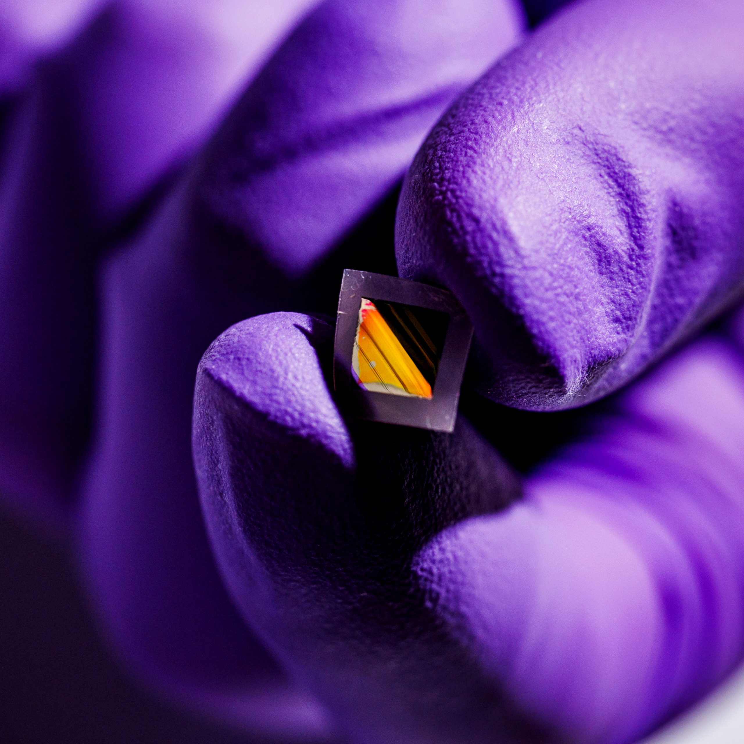
Utilizing their new technique, the team produced the thinnest pyroelectric membrane to date, at a thickness of 10 nanometers, and showcased that the film demonstrates high sensitivity to heat and radiation across the far-infrared range.
The recently engineered film could facilitate lighter, more versatile, and notably precise far-infrared (IR) detection devices, with possible uses in night-vision goggles and autonomous navigation in foggy weather. Current advanced far-IR sensors necessitate cumbersome cooling mechanisms. In contrast, the new pyroelectric thin film operates without cooling and is attuned to significantly smaller temperature variations. The researchers are seeking methods to integrate the film into lighter and more accurate night-vision eyewear.
“This film substantially diminishes weight and expense, rendering it lightweight, portable, and simpler to integrate,” states Xinyuan Zhang, a graduate researcher in MIT’s Department of Materials Science and Engineering (DMSE). “For instance, it could be directly worn on spectacles.”
The heat-sensitive film may also find applications in environmental and biological monitoring, in addition to imaging cosmic phenomena that emit far-infrared radiation.
Moreover, the innovative lift-off process is applicable beyond just pyroelectric substances. The researchers intend to utilize the technique to manufacture other ultrathin, high-performing semiconducting films.
Their findings are detailed today in a publication appearing in the journal Nature. The co-authors of the study from MIT include first author Xinyuan Zhang, Sangho Lee, Min-Kyu Song, Haihui Lan, Jun Min Suh, Jung-El Ryu, Yanjie Shao, Xudong Zheng, Ne Myo Han, and Jeehwan Kim, associate professor of mechanical engineering and materials science and engineering, along with researchers from the University of Wisconsin at Madison led by Professor Chang-Beom Eom and contributors from various other institutions.
Chemical Peel
Kim’s lab at MIT is discovering novel approaches to create smaller, thinner, and more adaptable electronics. They envision these ultrathin computing “coatings” being integrated into a range of devices, from smart contact lenses and wearable sensing textiles to flexible solar panels and bendable displays. To bring these devices to fruition, Kim and his team have been experimenting with methods to grow, peel, and layer semiconducting components, producing ultrathin, multifunctional electronic thin-film membranes.
One technique that Kim has pioneered is known as “remote epitaxy” — a method where semiconducting materials are cultivated on a single-crystalline substrate, interspersed with a very thin layer of graphene. The crystal framework of the substrate acts as a structure along which the new material can develop. The graphene functions as a nonstick layer, akin to Teflon, enabling researchers to easily peel off the new film and transfer it onto flexible and stacked electronic devices. After detaching the newly formed film, the original substrate can be reused for further thin film production.
Kim has employed remote epitaxy to create thin films with various attributes. In exploring different combinations of semiconducting materials, the researchers discovered that a particular pyroelectric substance, known as PMN-PT, did not need an intermediate layer to assist in detaching from its substrate. By simply growing PMN-PT directly on a single-crystalline substrate, researchers could remove the developed film without causing any damage to its delicate lattice.
“It performed surprisingly well,” Zhang remarks. “We found the peeled film is atomically smooth.”
Lattice Lift-off
In their recent investigation, the MIT and UW Madison teams closely examined the procedure and discovered that the material’s effective peeling property was facilitated by lead. Within its chemical structure, the team, along with colleagues from Rensselaer Polytechnic Institute, identified that the pyroelectric film possesses an organized configuration of lead atoms with considerable “electron affinity,” implying that lead attracts electrons and inhibits the charge carriers from migrating and connecting with other materials, such as an underlying substrate. This lead acts as tiny nonstick entities, allowing the entire material to detach seamlessly.
The researchers capitalized on this realization and created multiple ultrathin films of PMN-PT, each around 10 nanometers thick. They removed the pyroelectric films and transferred them onto a miniature chip to form an array containing 100 ultrathin heat-detecting pixels, each approximately 60 square microns (about .006 square centimeters). They exposed the films to increasingly slight temperature variations and observed that the pixels were exceptionally responsive to minute changes across the far-infrared range.
The responsiveness of the pyroelectric array is on par with that of leading-edge night-vision devices. These instruments currently rely on photodetector materials, in which temperature fluctuations cause the electrons within the material to leap in energy and briefly traverse an energy “band gap,” before returning to their baseline state. This electron transition serves as an electrical signal indicating the temperature change. However, this signal can be influenced by environmental noise, necessitating that photodetectors also incorporate cooling systems to bring their components down to liquid nitrogen temperatures.
Existing night-vision goggles and scopes are unwieldy and heavy. With the researchers’ new pyroelectric-based approach, NVDs could achieve similar sensitivity without the burden of cooling systems.
The team further discovered that the films exhibited sensitivity beyond the range of contemporary night-vision instruments and could respond to wavelengths throughout the entire infrared spectrum. This indicates that the films could be utilized in compact, lightweight, and portable devices for diverse applications necessitating various infrared regions. For example, when integrated within autonomous vehicle platforms, the films might enable cars to “see” people and other vehicles in complete darkness or under foggy and rainy conditions.
The film might also function in gas sensors for real-time and on-site environmental assessments, aiding in the detection of pollutants. In electronics, they could track heat variations in semiconductor chips to identify early signs of malfunctioning components.
The researchers assert that the new lift-off technique could be adapted to materials that may not inherently contain lead. In such instances, the team suspects that they could infuse Teflon-like lead atoms into the underlying substrate to replicate a similar peeling effect. For the moment, the team is diligently progressing towards the integration of pyroelectric films into a functioning night-vision system.
“We foresee that our ultrathin films could be developed into high-performance night-vision goggles, given their broad-spectrum infrared sensitivity at room temperature, which allows for a lightweight design devoid of a cooling mechanism,” Zhang states. “To transform this into a night-vision system, a functional device array should be coupled with readout circuitry. Moreover, testing in diverse environmental conditions is crucial for practical applications.”
This research received support from the U.S. Air Force Office of Scientific Research.