
“`html
As the necessity for more robust and efficient microelectronics systems escalates, the industry is embracing 3D integration — layering chips one atop another. This vertically organized framework could enable high-performance processors, such as those utilized for artificial intelligence, to be tightly packaged with other specialized chips for tasks like communication or imaging. However, technologists universally encounter a significant obstacle: preventing these stacks from overheating.
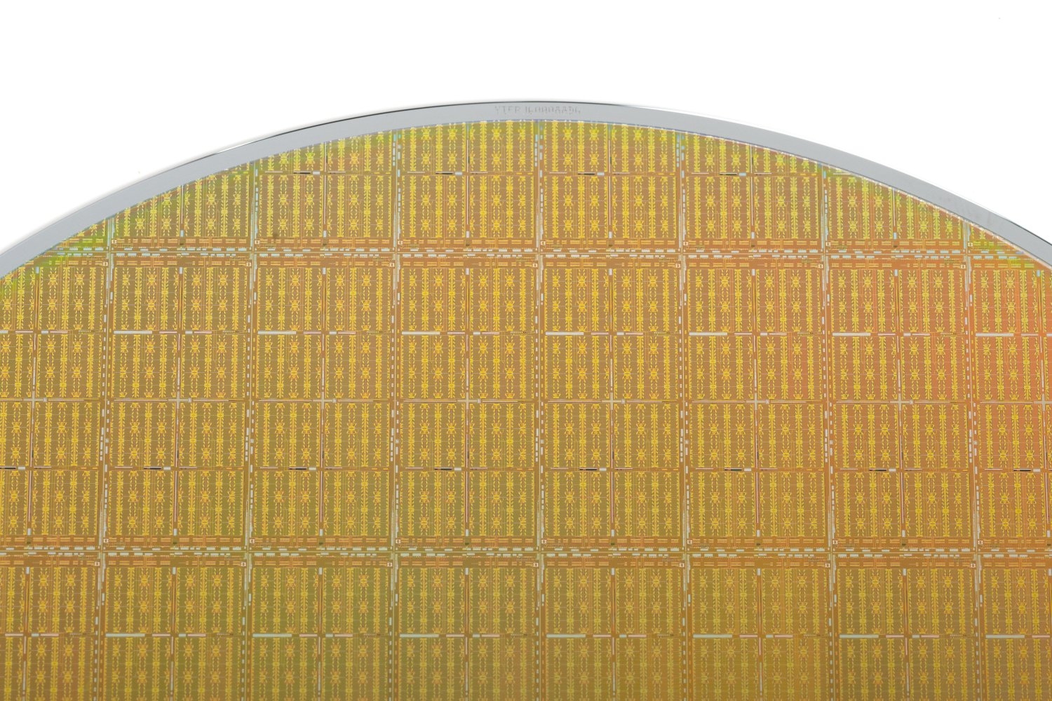
Recently, MIT Lincoln Laboratory has devised a specialized chip to evaluate and authenticate cooling strategies for stacked chip packages. The chip dissipates exceptionally high power, simulating high-performance logic chips, to produce heat via the silicon layer and in specific localized hot spots. Subsequently, as cooling technologies are implemented on the packaged stack, the chip records temperature fluctuations. When confined within a stack, the chip enables researchers to analyze heat distribution through stack layers and evaluate progress in maintaining their coolness.
“When dealing with just a single chip, it can be cooled from the top or bottom. But with multiple chips stacked, the heat has no means of escape. Current cooling methods do not allow the industry to stack multiple high-performance chips,” states Chenson Chen, who spearheaded the chip’s development alongside Ryan Keech, both from the laboratory’s Advanced Materials and Microsystems Group.
The benchmarking chip is currently employed at HRL Laboratories, a research and development firm co-owned by Boeing and General Motors, as they develop cooling systems for 3D heterogeneous integrated (3DHI) systems. Heterogeneous integration pertains to the stacking of silicon chips with chips made of other materials, such as III-V semiconductors used in radio-frequency (RF) systems.
“RF components can become exceedingly hot and operate at very high powers — adding an extra layer of complexity to 3D integration, which underscores the need for this testing capability,” Keech remarks.
The Defense Advanced Research Projects Agency (DARPA) financed the laboratory’s creation of the benchmarking chip to bolster the HRL program. This research evolves from DARPA’s Miniature Integrated Thermal Management Systems for 3D Heterogeneous Integration (Minitherms3D) initiative.
For the Department of Defense, 3DHI unveils new avenues for crucial systems. For instance, 3DHI could extend the range of radar and communication systems, facilitate the incorporation of advanced sensors on compact platforms like uncrewed aerial vehicles, or enable artificial intelligence data to be processed directly in deployed systems rather than in remote data centers.
The test chip was created through collaboration among circuit designers, electrical testing specialists, and technicians in the laboratory’s Microelectronics Laboratory.
The chip fulfills two roles: generating heat and detecting temperature. To produce heat, the team crafted circuits that could function at very high power densities, in the kilowatts-per-square-centimeter range, akin to the anticipated power demands of high-performance chips in the present and future. They also mirrored the layouts of circuits in those chips, allowing the test chip to function as a realistic substitute.
“We modified our existing silicon technology to essentially create chip-scale heaters,” notes Chen, who brings extensive experience in complex integration and chip design to the initiative. In the 2000s, he assisted the laboratory in pioneering the production of two- and three-tier integrated circuits, leading early advances in 3D integration.
The chip’s heaters simulate both the ambient heat levels within a stack and localized hot spots. Such hot spots frequently arise in the most buried and inaccessible regions of a chip stack, complicating efforts for 3D-chip developers to determine if cooling arrangements, like microchannels delivering cold fluids, are reaching those areas and proving sufficient.
This is where temperature-sensing components become essential. The chip is outfitted with what Chen describes as “tiny thermometers” that measure the temperature at multiple points across the chip as coolants are introduced.
These thermometers are essentially diodes, or switches that permit current to flow through a circuit when voltage is applied. As the diodes heat up, the current-to-voltage ratio alters. “We can assess a diode’s performance and determine that it’s at 200 degrees C, or 100 degrees C, or 50 degrees C, for instance,” Keech explains. “We creatively analyzed how devices could fail due to overheating and then leveraged those same properties to craft useful measurement instruments.”
Chen and Keech — along with other design, fabrication, and electrical testing specialists across the laboratory — are currently collaborating with HRL Laboratories researchers as they combine the chip with innovative cooling technologies and integrate those technologies into a 3DHI stack that could enhance RF signal power. “We need to dissipate heat equivalent to more than 190 laptop CPUs [central processing units], but within the dimensions of a single CPU package,” Christopher Roper, co-principal investigator at HRL, stated in a recent press release announcing their program.
According to Keech, the swift timeline for delivering the chip was a challenge surmounted through teamwork during all stages of the chip’s design, fabrication, testing, and 3D heterogeneous integration.
“Stacked architectures are viewed as the next frontier for microelectronics,” he asserts. “We aim to assist the U.S. government in advancing methods to integrate them effectively and achieve the highest possible performance for these chips.”
The laboratory team showcased this work at the annual Government Microcircuit Applications and Critical Technology Conference (GOMACTech), held March 17-20.
“`