

The process that unites new ferroelectric semiconductors forms a conductive channel that could facilitate high-power transistors

A novel category of semiconductors capable of retaining information in electric fields may lead to computers that consume less power, sensors with quantum-level accuracy, and the transformation of signals among electrical, optical, and acoustic modalities. However, the retention of two opposing electric polarizations within the same material remained an enigma.
Recently, a research team directed by engineers at the University of Michigan has unveiled the reason these materials, known as wurtzite ferroelectric nitrides, do not disintegrate.

“The wurtzite ferroelectric nitrides were recently identified and possess a wide array of applications in memory electronics, RF (radio frequency) technology, acousto-electronics, microelectromechanical systems, and quantum photonics, among other fields. Nevertheless, the fundamental mechanism behind ferroelectric switching and charge compensation has remained obscure,” stated Zetian Mi, the Pallab K. Bhattacharya Collegiate Professor of Engineering and co-corresponding author of the published study in Nature.
“What stabilizes the material? This remained largely unanswered.”
Electric polarization resembles magnetism; however, while a bar magnet has a north and south pole, an electrically polarized material features positive and negative poles. When these new semiconductors begin, they may exhibit polarization in one direction. When subjected to an electric field, the material’s polarization can flip—the positive pole becomes negative and vice versa—and when the electric field is removed, the altered polarization persists.
However, it’s usually not the entire material that changes polarization; instead, it separates into domains of original and reversed polarization. Where these domains converge, particularly when two positive ends meet, researchers were puzzled as to why the repulsion did not result in a physical rupture of the material.

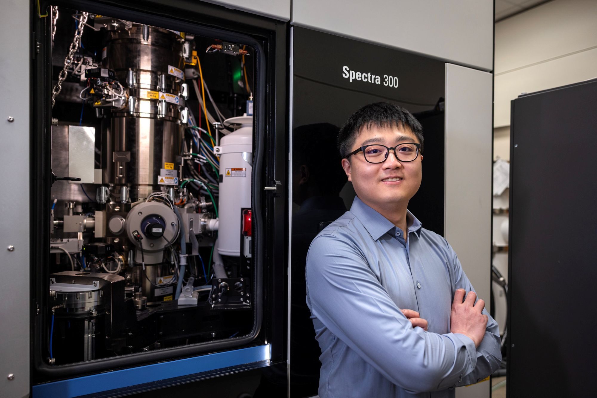
“Fundamentally, the polarization discontinuity is inherently unstable,” commented Danhao Wang, a U-M postdoctoral researcher in electrical and computer engineering and co-corresponding author of the study. “These interfaces possess a distinctive atomic configuration that has never been documented until now. Even more intriguingly, we discovered that this configuration could be ideal for conductive pathways in future transistors.”
Through experimental investigations spearheaded by Mi’s team and theoretical evaluations led by Emmanouil Kioupakis, a U-M professor of materials science and engineering, the researchers determined that an atomic-scale fracture exists in the material—but this fracture forms the adhesive that keeps it intact.

At the horizontal junction, where the two positive ends converge, the crystal framework is disrupted, leading to numerous dangling bonds filled with negatively charged electrons that perfectly counterbalance the surplus positive charge at the boundary of each domain within the semiconductor.
“This is a straightforward yet elegant finding—an abrupt change in polarization typically leads to undesirable defects, but in this situation, the resulting broken bonds supply exactly the charge necessary to stabilize the material,” remarked Kioupakis, who also holds the Karl F. and Patricia.
J. Betz Family Faculty Scholar and a co-corresponding author of the research.
“What’s impressive is that this charge neutralization isn’t merely a fortunate coincidence—it’s a direct outcome of the tetrahedral geometry,” he stated. “This renders it a universal stabilizing mechanism in all tetrahedral ferroelectrics—a category of materials that is quickly attracting interest for its prospective role in next-generation microelectronic devices.”
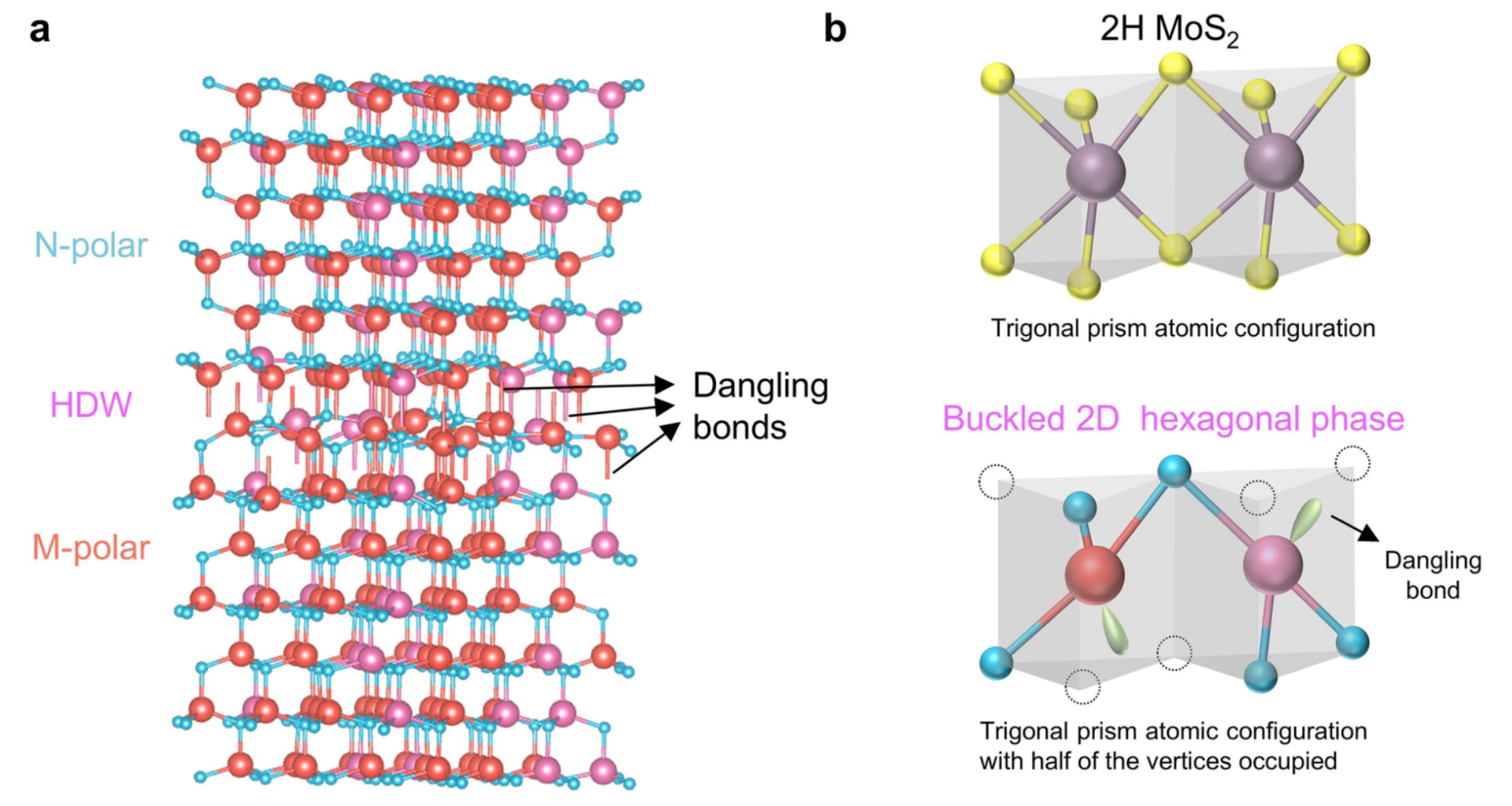
The research group revealed this using electron microscopy, which uncovered the atomic configuration of the specific semiconductor utilized, scandium gallium nitride. Where the domains converged, the typical hexagonal crystal structure was distorted over several atomic layers, resulting in the fractured bonds. The microscopy illustrated that the layers were more closely spaced than usual, but density functional theory calculations were necessary to disclose the dangling bond configuration.
Beyond maintaining the material’s integrity, the electrons in the dangling bonds establish an adjustable conduit for electricity along the junction, with approximately 100 times more charge carriers than in a standard gallium nitride transistor. This conduit can be activated or deactivated, repositioned within the material, and rendered more or less conductive by altering, relocating, enhancing, or diminishing the electrical field that determines the polarization.
The team quickly recognized its capability as a field effect transistor potentially able to handle substantial currents, making it suitable for high-power and high-frequency electronics. This is their next goal for development.
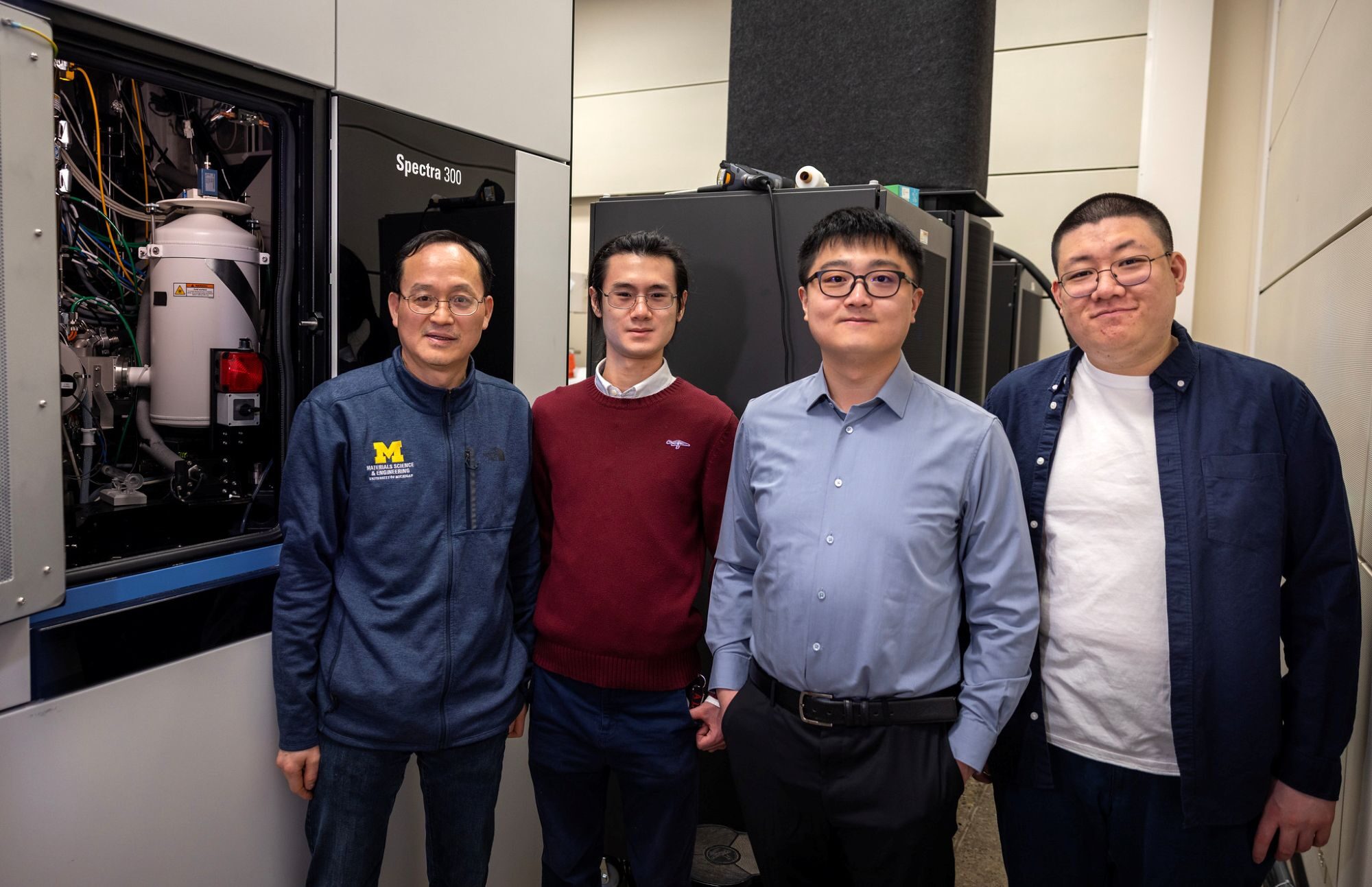
Danhao Wang is a co-first author of the research alongside U-M’s Ding Wang, a research fellow in electrical and computer engineering, and Mahlet Molla, a Ph.D. candidate in materials science and engineering. Researchers from McGill University in Canada also played a role in the study.
This research received funding from the National Science Foundation, Army Research Office, and U-M College of Engineering. Computational resources were supplied by the National Energy Research Scientific Computing Center, funded by the Department of Energy.
The device was fabricated in the Lurie Nanofabrication Facility and examined at the Michigan Center for Materials Characterization.
Mi also holds a professorship in electrical and computer engineering as well as materials science and engineering.
Written by Mena Davidson, College of Engineering