

“`html
More routes than previously imagined can result in optical topological insulators, substances with fascinating attributes that could have prospective uses in lasers, imaging devices, and beyond
The selection of engineered materials that may facilitate the next generation of advanced optical technologies—like lasers, sensors, and imaging devices—is significantly broader than previously acknowledged.
This assertion comes from recent findings at the University of Michigan, which investigated a category of materials known as topological insulators. These materials exhibit thrilling and adjustable characteristics regarding their energy and information transmission.
“We view this as a progression toward establishing a more adaptable and robust basis for future photonic technologies,” stated Xin Xie, a research fellow in the U-M Department of Physics and principal author of the new publication in the journal Physical Review X.
While these advanced materials might seem daunting, their fundamentals are relatively simple. In this context, the term insulator retains the same definition as in basic electronics: It denotes a substance that impedes the flow of something, such as wood or rubber in the case of electricity.
A topological insulator is essentially an insulator with a twist. While predominantly an insulator, it possesses a unique characteristic where its outer surface, regardless of its shape, is conductive. This feature opens new avenues for researchers to govern the flow of electricity or light for innovative applications.

The U-M team focused on a specific class of topological insulator that directs conduction to its edge while enabling unidirectional flow. There are similar materials under development in electronics, and researchers have shown interest in enhancing that performance for light, remarked Hui Deng, senior author of the study and professor of physics at U-M.
“There’s significant interest in these systems for transmitting photonic information,” she noted. “They facilitate unidirectional transport, allowing light to circumvent defects without scattering.”
It might be intuitive to think that, given the systems’ stringent performance requirements, the range of methods to create them would be somewhat exclusive. Contrary to this expectation, researchers have currently concentrated on just one method to achieve those properties with the assistance of an external magnetic field.
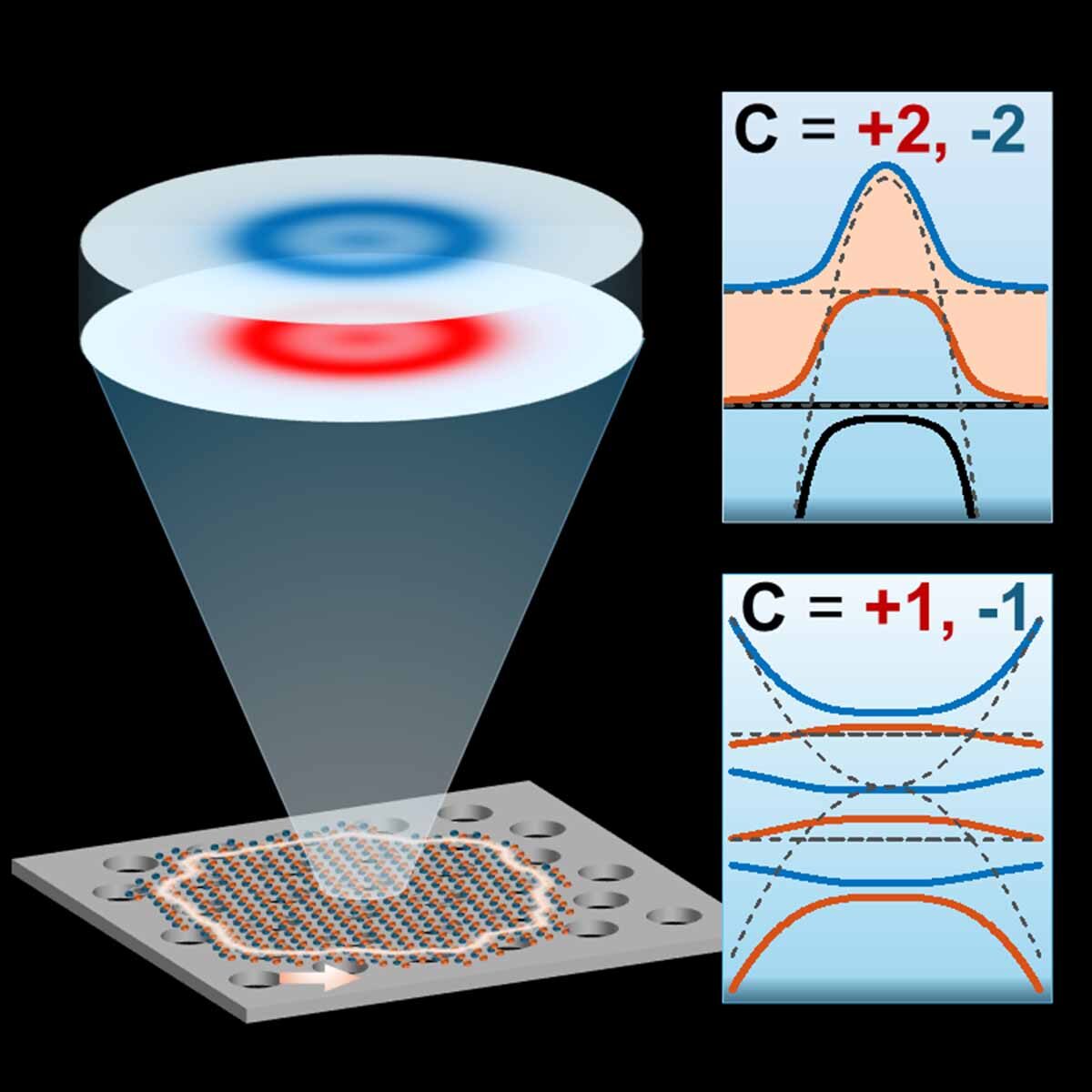
This primarily relates to a physical characteristic of the system referred to as its band gap. This can be envisioned as an energetic barrier within the system that must be surpassed for light or electrons to attain a conductive state.
The band gap of the topological insulator leads to its distinctive conductive traits. The dimension of a band gap also plays a crucial role. Larger band gaps enhance the “protection” of the unique edge conduction state, Deng stated.
Mirroring design principles from their electronic equivalents, scientists pursuing these photonic topological insulators had mainly targeted a singular type of band gap. However, the U-M team, which also included Kai Sun, professor of physics, employed symmetry analysis and computational simulations to explore alternative methods.
In electronics, the band structure is determined by the crystal arrangement of the material’s atoms. For optical devices, researchers design “photonic crystals” by creating arrays of pits, pillars, or other periodic nanoscale features that generate a system’s optical characteristics, including its band structure and band gap.
By linking specific designs of photonic crystals to atomically flat 2D materials, the team achieved the desired topological insulators, as indicated by their simulations. However, the simulated systems exhibited band structures that differed from the singular type previously emphasized.
This diversity implies that the design options for this category of topological insulators—termed polariton Chern insulators—are unexpectedly extensive, the researchers noted. For example, the team examined a type of photonic crystal that is already employed in various areas of optical research.
“What amazed me the most was how prevalent the necessary band structures actually are,” Xie remarked. “Even conventional photonic crystal designs—long utilized in other applications—can easily accommodate polariton Chern insulators, leading to significant performance improvements.”
The team’s next endeavor is to construct tangible examples of the systems they have simulated, which is a considerable challenge, but such experiments are a forte of Deng’s team. Once such a topological insulator is produced in a laboratory, the researchers estimate that its band gap could be up to approximately 100 times larger than the current record.
This research received funding from the Army Research Office, Air Force Office of Scientific Research, Office of Naval Research, National Science Foundation, and the Gordon and Betty Moore Foundation. The study was made possible through the Advanced Research Computing Core at U-M and its Great Lakes high-performance computing cluster.
“`