
“`html
The sophisticated semiconductor compound gallium nitride is expected to be crucial for the upcoming generation of rapid communication systems and the power electronics required for cutting-edge data centers.
Unfortunately, the steep expense of gallium nitride (GaN) and the expertise needed to integrate this semiconductor compound into conventional electronics have constrained its adoption in commercial sectors.
Now, investigators from MIT and other institutions have created a novel manufacturing technique that incorporates high-performance GaN transistors onto standard silicon CMOS chips in an economical and scalable manner, as well as being compatible with existing semiconductor fabrication facilities.
Their approach entails constructing numerous minuscule transistors on the surface of a GaN chip, individually excising each transistor, and then adhering only the requisite number of transistors onto a silicon chip via a low-temperature procedure that maintains the functionality of both materials.
The expense remains low since a minimal quantity of GaN material is added to the chip, yet the resultant device can experience a significant performance increase from compact, high-speed transistors. Additionally, by distributing the GaN circuit into discrete transistors across the silicon chip, the innovative technology can also lower the overall system temperature.
The researchers utilized this process to manufacture a power amplifier, a critical component in mobile phones, that achieves greater signal strength and efficiency compared to devices with silicon transistors. In a smartphone, this could enhance call quality, increase wireless bandwidth, improve connectivity, and prolong battery life.
As their technique aligns with standard methods, it could enhance current electronics as well as future technologies. In the future, the new integration strategy could even facilitate quantum applications, as GaN outperforms silicon at the cryogenic temperatures vital for various quantum computing forms.
“If we can reduce the cost, enhance scalability, and simultaneously boost the performance of the electronic device, it’s obvious that we should embrace this technology. We’ve merged the advantages of silicon with the finest gallium nitride electronics. These hybrid chips have the potential to transform several commercial sectors,” states Pradyot Yadav, an MIT graduate student and lead author of a publication about this method.
He is accompanied in the publication by fellow MIT graduate students Jinchen Wang and Patrick Darmawi-Iskandar; MIT postdoctoral researcher John Niroula; senior authors Ulriche L. Rodhe, a visiting scientist at the Microsystems Technology Laboratories (MTL), and Ruonan Han, an associate professor in the Department of Electrical Engineering and Computer Science (EECS) and a member of MTL; plus Tomás Palacios, the Clarence J. LeBel Professor of EECS and director of MTL; as well as collaborators from Georgia Tech and the Air Force Research Laboratory. The research was recently showcased at the IEEE Radio Frequency Integrated Circuits Symposium.
Exchanging transistors
Gallium nitride stands as the second most extensively employed semiconductor globally, following silicon, and its distinctive characteristics render it suitable for applications including lighting, radar systems, and power electronics.
The material has existed for decades, and to access its optimal performance, it is crucial for GaN chips to be linked to digital chips made of silicon, known as CMOS chips. To facilitate this, some integration methods bond GaN transistors onto a CMOS chip by soldering the connections, but this restricts how minuscule the GaN transistors can be. Smaller transistors allow for increased operational frequencies.
Alternative methods integrate an entire gallium nitride wafer atop a silicon wafer, but utilizing such a substantial amount of material is exceedingly expensive, particularly since only a few tiny transistors are needed from the GaN. The remaining material in the GaN wafer is rendered superfluous.
“We aimed to merge the capabilities of GaN with the processing power of silicon-based digital chips, without compromising on either cost or bandwidth. We accomplished this by integrating ultra-tiny discrete gallium nitride transistors directly onto the silicon chip,” Yadav elucidates.
The innovative chips result from a multi-step procedure.
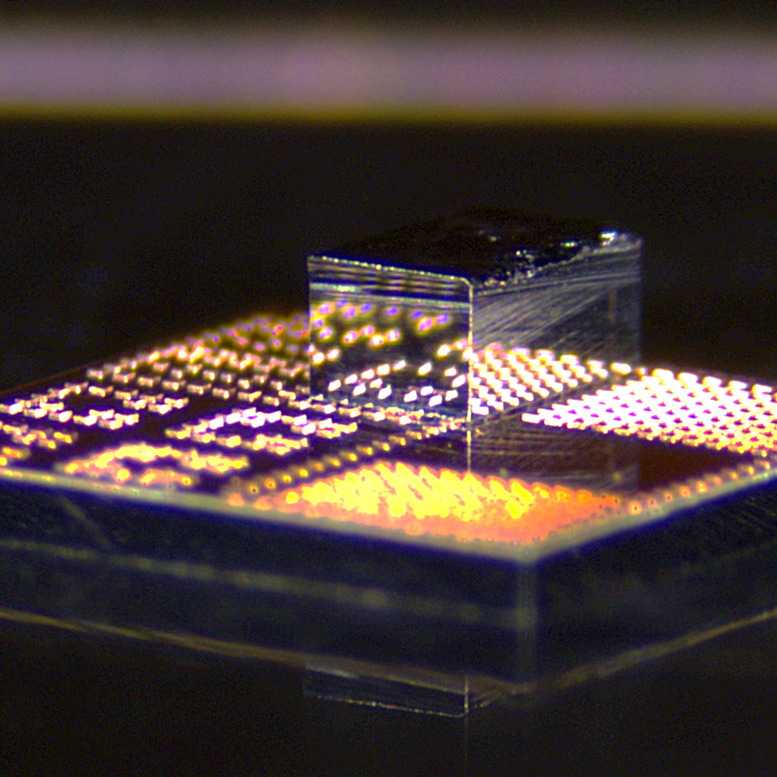
Initially, a densely arranged cluster of tiny transistors is fabricated over the entire area of a GaN wafer. Using very precise laser technology, they trim each one down to the dimensions of the transistor, which is 240 by 410 microns, crafting what they refer to as a dielet. (A micron constitutes one millionth of a meter.)
Each transistor is manufactured with minuscule copper pillars on top, which they utilize to bond directly to the copper pillars on the surface of a standard silicon CMOS chip. Copper-to-copper bonding can occur at temperatures below 400 degrees Celsius, which is sufficiently low to evade damage to either material.
Current GaN integration techniques necessitate bonds that employ gold, a costly material that requires much higher temperatures and stronger bonding forces than copper. Given that gold can contaminate the tools used in most semiconductor fabrication facilities, it generally demands specialized environments.
“We sought a method that was low-cost, low-temperature, and low-force, and copper excels in all these aspects compared to gold. Simultaneously, it boasts superior conductivity,” Yadav asserts.
A novel tool
To facilitate the integration process, they developed a specialized new instrument that can meticulously integrate the extraordinarily tiny GaN transistor with the silicon chips. The tool employs a vacuum to secure the dielet as it navigates above a silicon chip, accurately aligning with the copper bonding interface with nanometer precision.
They applied advanced microscopy to oversee the interface, and when the dielet is perfectly positioned, they apply heat and pressure to bond the GaN transistor to the chip.
“For each step in the process, I had to find a new collaborator with expertise in the necessary techniques, learn from them, and then assimilate that into my platform. It was two years of relentless learning,” Yadav mentions.
Once the researchers had refined the fabrication process, they showcased it by developing power amplifiers, which are radio frequency circuits that amplify wireless signals.
Their devices achieved higher bandwidth and enhanced gain compared to devices constructed with traditional silicon transistors. Each compact chip occupies an area of less than half a square millimeter.
Furthermore, because the silicon chip used in their demonstration is based on Intel 16 22nm FinFET state-of-the-art metallization and passive options, they were able to incorporate components frequently utilized in silicon circuits, such as neutralization capacitors. This considerably improved the gain of the amplifier, advancing it closer to facilitating the next generation of wireless technologies.
“In addressing the slowdown of Moore’s Law in transistor scaling, heterogeneous integration has emerged as a promising remedy for continued system scaling, minimized form factor, improved power efficiency, and cost optimization. Especially in wireless technology, the cohesive integration of compound semiconductors with silicon-based wafers is essential for realizing unified systems of front-end integrated circuits, baseband processors, accelerators, and memory for next-generation antennas-to-AI platforms. This work marks a significant milestone by showcasing 3D integration of multiple GaN chips with silicon CMOS and extends the boundaries of current technological limits,” comments Atom Watanabe, a research scientist at IBM who was not part of this paper.
This work is partially funded by the U.S. Department of Defense through the National Defense Science and Engineering Graduate (NDSEG) Fellowship Program and CHIMES, one of the seven centers in JUMP 2.0, a Semiconductor Research Corporation initiative by the Department of Defense and the Defense Advanced Research Projects Agency (DARPA). Fabrication was conducted using facilities at MIT.Nano, the Air Force Research Laboratory, and Georgia Tech.
“`